


If you think of a single atom as a grain of sand, then a wavelength of visible light—thousands of times larger than an atom’s width—is comparable to an ocean wave. This vast size difference has long prevented scientists from using optical microscopes to see individual atoms. However, a groundbreaking technique developed by MIT researchers is changing that narrative.
In a paper published today in Nature Communications, MIT scientists unveiled a new computational method that enables optical microscopes to resolve individual atoms within a crystal structure. This method, known as the “discrete grid imaging technique” or DIGIT, leverages computational imaging to calculate the most probable location of individual atoms based on the material’s known atomic configuration.
Breaking the Diffraction Limit
Historically, the diffraction limit has been a significant barrier to optical microscopy, preventing the resolution of features smaller than half the wavelength of visible light—about 200 to 300 nanometers. Super-resolution microscopy, a technique awarded the Nobel Prize in Chemistry in 2014, has enabled scientists to visualize features as small as 10 nanometers by using laser light at specific frequencies to resonate with target molecules.
Despite these advancements, individual atoms remained elusive to optical microscopes, which are simpler and less expensive than electron microscopes. The introduction of DIGIT, however, represents a significant leap forward.
How DIGIT Works
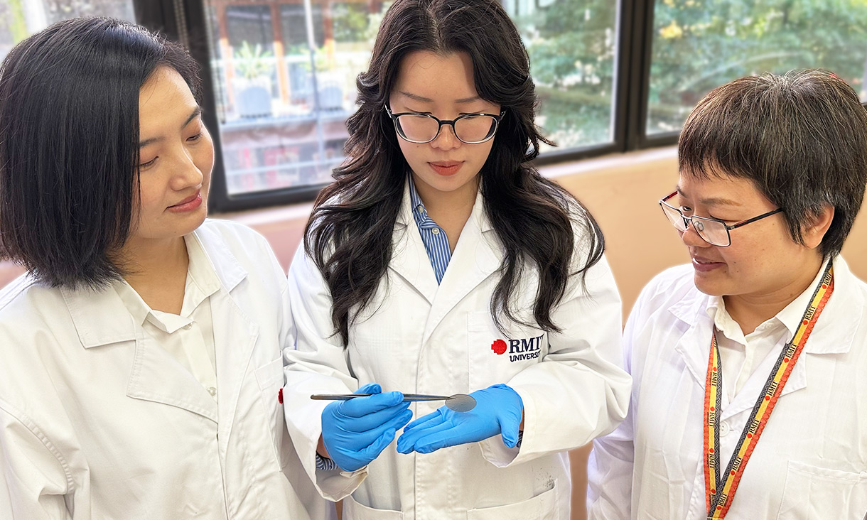
Lead author Yuqin “Sophia” Duan, a graduate student at MIT, explains that DIGIT uses a known atomic layout as a map to determine the precise location of atoms. “It’s like you know there’s a seating chart,” Duan says. “Previous methods could tell you what section an atom is in. But now we can pinpoint exactly which seat the atom is in.”
With DIGIT, the team can pinpoint individual atoms with a resolution of 0.178 angstroms, enabling optical microscopes to localize atomic-scale features in materials with known atomic patterns, such as crystalline materials or proteins with repeating molecular chains.
Applications and Implications
The potential applications of DIGIT are vast. It could guide the design of quantum devices, which often require precise placement of individual atoms within a crystal. Beyond quantum technologies, DIGIT can provide new insights into how defects and impurities influence the behavior of advanced materials, from semiconductors to superconductors.
Duan’s co-authors at MIT include Qiushi Gu, Hanfeng Wang, Yong Hu, Kevin Chen, Matthew Trusheim, and EECS Professor Dirk Englund. Their collaborative efforts have opened new possibilities for optical microscopy, traditionally limited by the diffraction limit.
Scientific Context and Future Directions
Traditionally, scientists have used transmission or scanning electron microscopes to image features smaller than a nanometer. These methods, while effective, require high-energy beams and vacuum conditions, making them unsuitable for delicate biological specimens. Optical microscopes, on the other hand, operate at lower energies and are safe for biological samples but have been limited by the diffraction limit.
By incorporating the physical configuration of materials into imaging techniques, DIGIT offers a new approach. “No one has ever done this before, to include the physical constraints or system information into the resolution technique,” Duan notes.
To test their method, the researchers used a diamond sample, replacing some carbon atoms with silicon atoms. By applying DIGIT, they could precisely locate the silicon atoms within the diamond lattice, achieving the sharpest resolution of any optical-based imaging technique.
“It’s a big step—it takes optical microscopes into the realm of atomic scale, something people thought only electron microscopes or X-rays could do,” Duan says. “That opens up a whole new way of studying materials and biology.”
The team has made the DIGIT code available on GitHub, encouraging scientists worldwide to apply it to their optical measurements, provided their sample has a well-understood atomic structure. This accessibility could lead to new discoveries in material science and biology, as researchers begin to see finer details using light.
As this innovative method gains traction, it promises to transform the landscape of microscopy, offering new insights into the atomic world and beyond.