


The potential use of low-energy light to shape ferroelectric thin films for micro-devices is advancing with an international team of researchers recently reporting success with ‘photostriction’. This development, led by Flinders University, marks a significant step forward in the field of optomechanics and wireless, light-powered sensors.
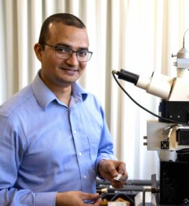
Light-induced nonthermal deformation of materials, or photostriction, has the advantage of directly converting photon energy into mechanical motion. According to Dr. Pankaj Sharma, a researcher at Flinders University, this offers exciting possibilities for the future of micro-devices. “Light can precisely control the internal structure and electronic responses of these films,” Dr. Sharma explains, pointing to a future where micro-devices can be powered and actuated entirely by light.
Challenges and Innovations in Photostriction
Since its discovery in the 1960s, scientists have explored photostriction in a wide range of materials, including semiconductors, oxides, ferroelectrics, and polymers. However, many of these systems face significant challenges. “Conventional semiconductors show weak responses, lead-based materials raise environmental concerns, and some light-sensitive compounds are unstable,” notes Dr. Sharma, the lead and corresponding author of the new article in ACS Nano, a journal of the American Chemical Society (ACS).
Ferroelectrics, often referred to as the electrical analogues of magnets, show promise but are mostly limited to UV light. Additionally, epitaxial thin films grown on substrates are constrained by their supports. However, the research team has now demonstrated major photostrictive effects under visible light in unconstrained thin films of BiFeO3 – a multiferroic material.
Breakthrough with BiFeO3 Films
BiFeO3, or bismuth ferrite, is an inorganic compound with a perovskite structure that is a room-temperature multiferroic material. This means it exhibits both ferroelectric and antiferromagnetic properties, making it a promising candidate for new electronic and spintronic devices, as well as for applications like photocatalysis and energy storage.
The study published in ACS Nano reveals that these nanostructured films, created through a low-cost, scalable spray-pyrolysis process, exhibit record-high light-driven strains using remarkably low optical power. “The resulting photostriction is up to five times greater than bulk BiFeO3 crystals, rivalling advanced halide perovskites but without their stability or toxicity issues,” explains Dr. Haoze Zhang, a postdoctoral fellow and first author of the study at Flinders University.
“These materials could form the foundation for light-controlled actuators, wireless sensors, and self-powered optomechanical systems,” says Dr. Zhang. “The key lies in unconstrained nanocrystalline BiFeO3 films, which feature a dense network of domain walls – atomically thin boundaries within the crystal.”
Implications for Future Technologies
By tuning light wavelength and intensity, the research team demonstrated fine control over piezoelectric and ferroelectric properties, establishing a versatile platform for energy-efficient, multifunctional nanoscale devices. This breakthrough could pave the way for significant advancements in the development of light-powered technologies.
The paper, titled ‘Giant Photostriction and Optically Modulated Ferroelectricity in BiFeO3’ (2025), was authored by H. Zhang, M.C. Nagashree, R.F. Webster, J. Edwards, B.V. Rajendra, S.D. Kulkarni, T. Yousaf, D. Zhang, A. Gruverman, J. Seidel, and P. Sharma. It has been published in ACS Nano, DOI: 10.1021/acsnano.5c05203. The authors hail from institutions including Flinders University, UNSW Sydney, Manipal Academy of Higher Education (India), and the University of Nebraska-Lincoln.
Funding for this research was supported by the Australian Research Council Discovery Projects (DP240102137, DP240100238), the Australian National Fabrication Facility (ANFF), Flinders University, and the ARC Centre of Excellence in Future Low-Energy Electronics Technologies (FLEET).
This breakthrough represents a significant leap forward in the field of nanotechnology and photostriction, with potential applications that could transform the landscape of micro-device technology.