


Lawrence Livermore National Laboratory (LLNL) engineers, in partnership with Stanford University, have unveiled a groundbreaking 3D nanofabrication method that could transform two-photon lithography (TPL) from a slow, laboratory-based technique into a scalable manufacturing process. This advancement, published today in Nature, utilizes a novel TPL platform leveraging large arrays of engineered metalenses to significantly increase production speed without compromising precision.
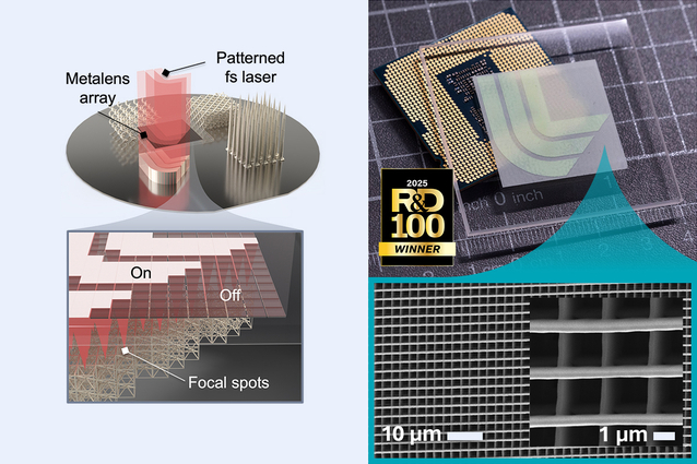
The innovative platform splits a femtosecond laser into over 120,000 coordinated focal spots, enabling simultaneous writing across centimeter-scale areas. This metalens-based approach achieves intricate 3D architectures with minimum feature sizes of 113 nanometers and boosts throughput by more than a thousand times compared to existing commercial systems.
“When the 3D printing system started to work at one-centimeter scale and then three-centimeter scale for the first time, it was really amazing to see the idea that was developed for three to four years at that time come true,” said Xiaoxing Xia, an LLNL materials engineer and principal investigator. “To see a print being done accurately at speed hundreds to thousands of times faster than our commercial printer, we realized a breakthrough has happened.”
From Laboratory to Industry: Scaling Nanofabrication
Historically, TPL has been prized for its nanoscale resolution, but its application was limited by the need for microscope objectives, which restricted printable areas to a few hundred microns. Larger areas required stitching numerous tiles together, a time-consuming process prone to alignment errors.
The team’s metalens TPL approach replaces traditional microscope objectives with a tiled array of high-numerical-aperture metalenses, each functioning as a miniature printer. Instead of scanning a single beam, the system prints thousands of small regions in parallel, merging them seamlessly in a single pass. This method avoids the proximity effects that hindered earlier multi-beam approaches.
“It means TPL finally has the potential for industry adoption,” said Songyun Gu, a postdoctoral researcher at LLNL and the first author of the study.
“With wafer-scale nanomanufacturing, we have the potential to make nanomaterials and microdevices the same way we make computer chips, which are highly complex but can be made in volume at very low unit cost. And meta-optics is exactly the solution.”
Adaptive Light Control: Expanding Design Possibilities
The team introduced a spatial light modulator to print non-periodic structures, allowing real-time adjustments to the intensity of each focal spot. This system can switch beams on or off, tune linewidths with grayscale control, and choreograph beams to form larger patterns layer by layer. Initially intended to equalize beam intensity, this capability unexpectedly unlocked extensive design freedom.
“During the project, we realized that by dynamically switching the focal spots on and off and carefully planning the printing trajectory, we can actually print fully stochastic structures with a high degree of parallelization,” Xia explained. The team named the method Adaptive Meta-Lithography, acknowledging support from LLNL’s Advanced Manufacturing Laboratory.
This parallel yet adaptive approach allows metalens TPL to fabricate a wide range of products, from gradient density laser targets to flexible terahertz devices, and even tens of millions of micro-particles per day. It also facilitates the creation of complex modular architectures for emerging technologies in microfluidics, quantum information, microelectronics, photonics, fusion energy, and biomedicine.
Future Prospects and Industry Impact
As higher-power lasers, larger metalens wafers, and faster modulators become available, the team anticipates that metalens TPL will print even more complex devices at greater speeds, steering 3D nanomanufacturing toward mainstream, wafer-scale production. This technology platform, named MetaLitho3D, recently received a 2025 R&D 100 Award, highlighting its potential for industry adoption to solve real-world problems.
Xia envisions the convergence of optics and additive manufacturing as a pivotal advancement for the field.
“Light is the finest chisel on earth to craft functional materials and micro-architectures,” he said. “New ways to control light will revolutionize how to make materials.”
The research team includes LLNL’s Anna Guell Izard, Dongping Terrel-Perez, Sijia Huang, Travis Massey, Alex Abelson, Magi Mettry-Yassa, Wonjin Choi, and Thejaswi Umanath Tumkur; Stanford’s Chenkai Mao, You Zhou, and Jonathan Fan; and Caltech’s Wenjie Zhou, Hujie Yan, Ziran Zhou, and Chiara Daraio.