


As the microelectronics industry embraces gate-all-around transistor designs for next-generation smartphones, a groundbreaking approach first demonstrated nearly 20 years ago at Lawrence Berkeley National Laboratory (Berkeley Lab) is garnering renewed attention. This innovative technology, known as gate-all-around field-effect transistors (GAA-FET), represents a significant architectural advancement, enabling the integration of billions more transistors into the microchips that power smartphones and laptops.
The “gate-all-around” design enhances control over the transistor channel, resulting in improved performance and reduced power consumption. While the industry is now adopting GAA-FET through traditional top-down fabrication methods, Berkeley Lab’s early bottom-up approach highlighted the potential of this geometry through chemical synthesis.
Revisiting a Pioneering Approach
Peidong Yang, a faculty senior scientist at Berkeley Lab’s Materials Sciences Division and a professor at UC Berkeley, expressed enthusiasm for the ongoing evolution of transistor architectures. “I’m pleased to see the continued evolution of transistor architectures in the semiconductor industry,” Yang stated. His pioneering work on the bottom-up synthesis of gate-all-around structures, published in 2006, demonstrated alternative pathways for fabricating these complex geometries.
Transistors, the fundamental building blocks of modern computing, are integral to the performance of microchips found in today’s smartphones, which can contain over 10 billion transistors, each measuring just 5 nanometers. Acting as switches, transistors control the flow of current through a semiconductor channel, enabling the binary operations essential to modern computing.
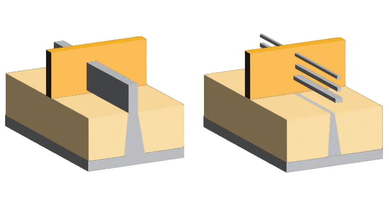
The Transition from FinFET to GAA-FET
For the past decade, the FinFET (Fin Field-Effect Transistor) design has dominated, with its vertical semiconductor channel resembling a fin and the gate wrapping around it on three sides. However, as FinFETs shrink below 5 nanometers, they encounter challenges in gating and energy efficiency.
Microchip manufacturers are determined to push the boundaries of Moore’s Law by packing even more transistors into a chip no larger than a fingernail. Achieving higher transistor density necessitates smaller transistors, potentially down to 2 nanometers—the size of a DNA strand—or even 1 nanometer, equivalent to a few silicon atoms. Smaller chips not only enable smaller devices but also enhance energy efficiency.
The Promise of Gate-All-Around Design
The microelectronics industry has long recognized the potential of the gate-all-around approach—a design that fully encases the channel with the gate—to create higher-performing, more efficient transistors at sub-5-nanometer scales. Although traditional top-down lithography faced challenges in fabricating GAA-FET geometries in the early 2000s, researchers explored various approaches to realize this design concept.
In a scientific first, Yang’s group demonstrated an unconventional bottom-up approach to creating silicon-based, gate-all-around transistors using chemical vapor deposition (CVD). Their seminal 2006 paper in Nano Letters, titled “Silicon Vertically Integrated Nanowire Field Effect Transistors,” detailed the use of CVD to grow vertical silicon nanowires coated with an ultrathin metallic layer, embedded in silicon dioxide. This achieved a gate-all-around structure using industry-standard materials through chemical synthesis rather than traditional lithography.
“It’s fascinating to see how semiconductor technology has evolved over the past two decades,” Yang remarked. “Our early work exploring different approaches to transistor design was part of the broader research community’s efforts to advance microelectronics.”
Impact and Industry Adoption
Yang’s work demonstrated the fundamental viability of the GAA-FET architecture when many considered it merely theoretical. By successfully creating functional gate-all-around structures through CVD, the Berkeley Lab team validated the superior electrostatic control that would later motivate industry adoption. This early proof-of-concept work helped establish that complete gate wrapping could indeed deliver the performance improvements that theory predicted, providing confidence for the substantial R&D investments that followed.
Today, as microchip manufacturers embrace the gate-all-around concept, they are achieving the architecture through top-down fabrication approaches. The move represents a significant step forward in the quest for more efficient and powerful microchips, paving the way for the next generation of electronic devices.
Looking Ahead
The implications of this technological evolution are profound. As the industry continues to refine and implement GAA-FET designs, the potential for smaller, more efficient, and more powerful devices grows. This development not only promises to enhance the capabilities of smartphones and laptops but also holds the potential to revolutionize other sectors reliant on microelectronics, from automotive to healthcare.
As researchers and manufacturers continue to explore the limits of transistor miniaturization, the pioneering work at Berkeley Lab serves as a testament to the power of innovative thinking and the enduring impact of foundational research. The journey from concept to widespread adoption underscores the importance of early-stage exploration in shaping the future of technology.